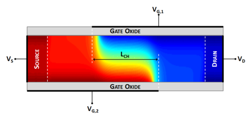
Ultimate Device Scaling
Single-layer MoS2 transistors
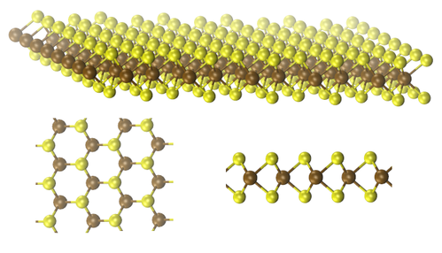
Molybdenum disulfide (MoS2) monolayer is a direct bandgap semiconductor with a relatively large (1.8 eV) gap, and with a high (around 200 cm^2/Vs) electron mobility. These properties along with the excellent electrostatic control the two-dimensional structure offers, make single-layer MoS2 a promising candidate for next generation nanotransistors' material. It has also started attracting a lot of attention as active component of flexible electronic circuits. The goal of this project is to investigate electronic and thermal transport in MoS2 transistors in the framework of three-dimensional, atomistic, full-band quantum transport simulations, based on the empirical tight-binding and valence-force-field methods. Armed with state-of-the-art simulation models, a better insight into the physical mechanisms governing 2-D MoS2 field-effect transistors is expected.
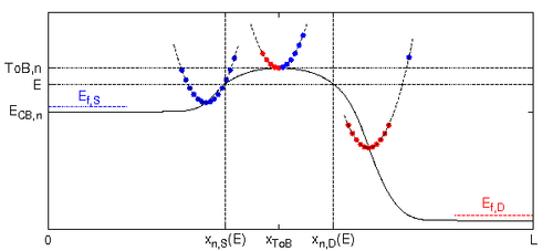
Under-the-barrier model
This model was developed in order to investigate the performance of ultra-scaled nanowire FETs in a numerically very efficient way. The goal was to implement a method that reduces the heavy computational burden associated with 3-D atomistic quantum-transport simulations, while keeping the accuracy even when gate lengths are shrinked below 10 nm. At this scale source-to-drain (intra-band) tunneling plays a significant role in the electron transport. To capture this current contribution, the Wentzel-Kramers-Brillouin approximation was used. The mean position-dependent charge-density and electrostatic potential in the device along the transport axis was determined self-consistently in the Top-of-the-Barrier picture, and by using the gradual channel approximation when solving the Poisson-equation. Excellent agreement was found when comparing simulation results with atomistic simulations, while the computational time was decreased with several orders of magnitudes. The method made it available to investigate efficiently the diameter-, gate length-, and transport direction dependence of the performance of both n- and p-type Si, Ge, and InAs nanowire FETs.
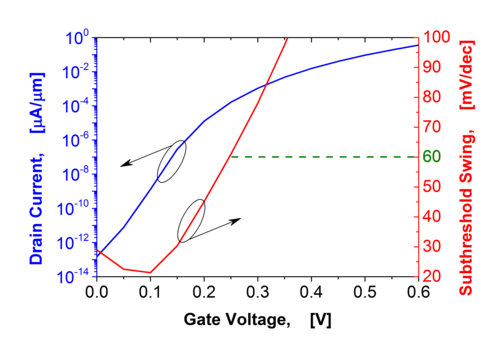
Interband Tunneling-Based Low-Power Devices
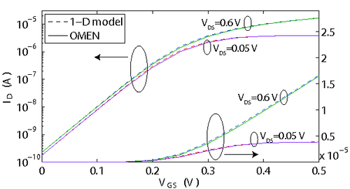
The alarming growth of power consumption by electronic devices, ranging from mobile phones to laptops to televisions to supercomputers, is the greatest challenge of today's nanoelectronics. To address this issues, studies should focus on increasing transistors energy efficiency and virtually eliminate their power consumption when they are in passive or standby mode. In this scenario, one of the candidates with the highest potential for low-power circuits and systems is represented by the Tunnel-FET (TFET). TFETs are steep slope switches that thanks to a different injection mechanism with respect to conventional transistors are able to to reduce the subthreshold swing of their transfer characteristic even below the theoretical limit of the 60mV/dec dictated by the thermionic emission. In particular, in these novel devices the injection of the charge in the channel is not governed by the control of an emission barrier like in conventional MOSFETs, but by the quantum?mechanics crossover of the barrier: this results in an off-on switching transition that can be smaller than the physical limit dictated by the Maxwell?Boltzmann statistics. To achieve the full potential of TFETs, however, it is required to properly understand the physics governing their working principle. Being inherently based on quantum mechanics, an accurate study requires ad-hoc tools able to catch all the physical mechanisms at their smallest dimension scale. To this purpose we are using the atomistic simulator OMEN, that is credited to be the most advanced simulator tool worldwide developed, to study all the fundamental aspects and material and architectural parameters affecting TFETs behavior. Both research and industry consider this as a fundamental step towards the establishment of a comprehensive modeling and simulation environment for being able to optimize the device performance and fully exploit the TFET transistors on device and and system level for novel energy efficient integrated circuits.