A collaboration with researchers at UT Austin, now published in Nature Materials!
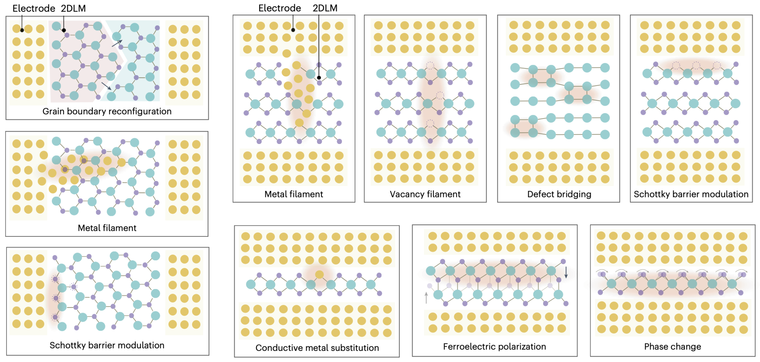
By sandwiching a semiconducting or insulating layer between two metallic electrodes and applying an electric field, its resistance can be changed by factors sometimes larger than 1000. A reverse electric field then brings it back to its original value. This property has been likened to dielectric breakdown, and used to make electronic memory devices.
While this effect has been previously observed in a variety of relatively thick materials, typically encountered in semiconductor manufacturing, it has recently also been detected in two-dimensional (2D) materials, a promising platform for future nanoelectronic technologies. Since the discovery of resistive switching in ultra-thin 2D compounds, a question has remained open regarding their functionality: what kind of atomic movements can trigger orders of magnitude resistance changes in materials whose thickness does not exceed 0.5 nm? Together with collaborators at UT Austin, we therefore investigated the origin of resistance switching in 2D materials.
We combined hints from experimental imaging studies and theoretical insights from ab-initio simulations to address this question. Our findings are now presented in a review article that distills a large volume of prior research into 2D resistive-switching devices down into a consistent, atomistic picture of the physical mechanisms involved. We address how these mechanisms can be harnessed in the form of nano-devices for applications in next-generation computer memory and communication technology.
See the article in Nature Materials!: external page https://www.nature.com/articles/s41563-025-02170-5